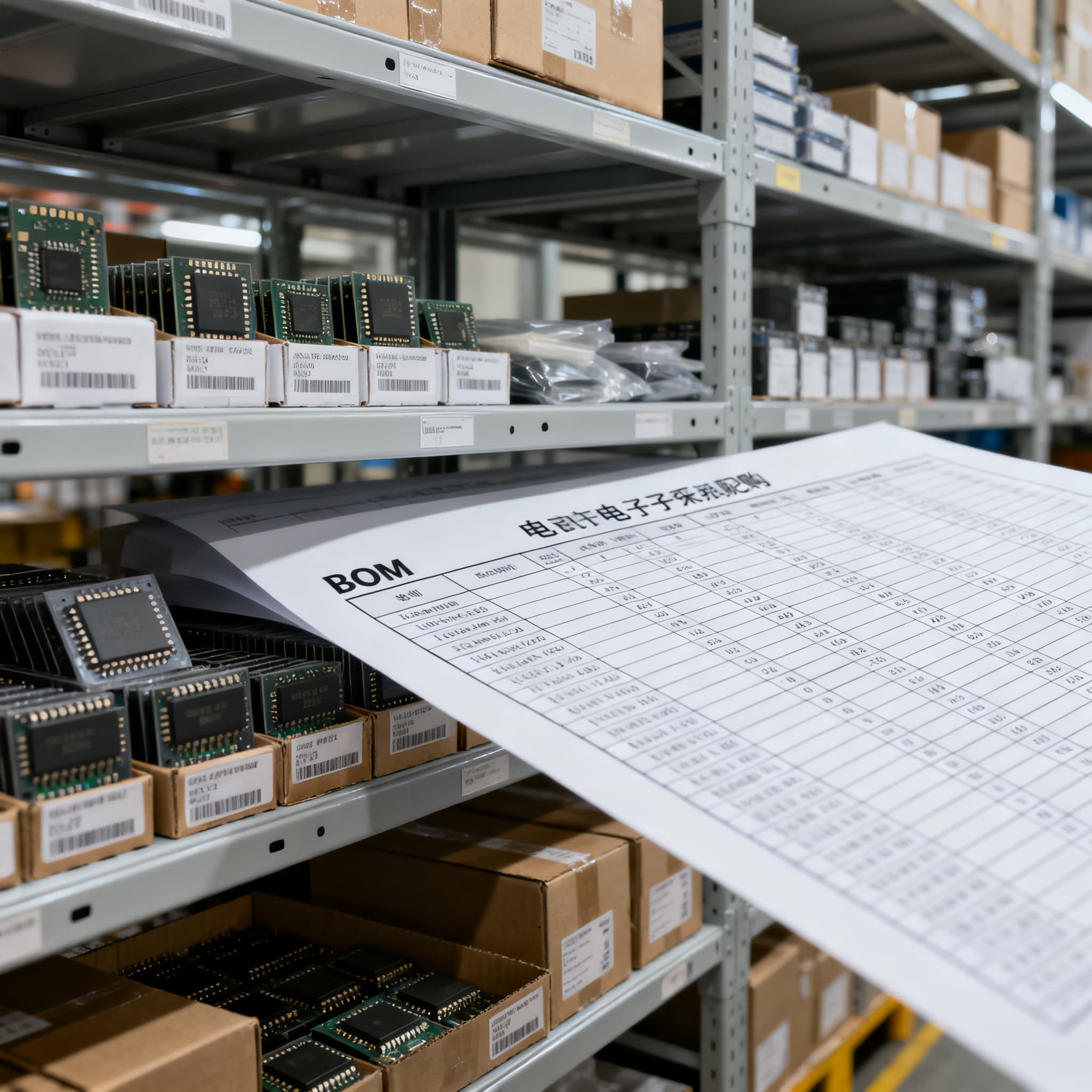
FDV301N Datasheet Specs Buyers Should Verify Before RFQ
FDV301N procurement checklist: datasheet specs and pinout fields to verify on RFQ, plus BOM upload path on BOMNow.
Why the FDV301N's Lifecycle Status Is a Pre‑RFQ Red Flag
When procurement teams receive a BOM line calling out the FDV301N, the instinct is often to fire off three RFQs and compare landed cost. That shortcut can backfire with small-signal MOSFETs that have been in circulation for decades. The FDV301N — an N‑Channel logic‑level FET originally introduced by Fairchild Semiconductor and now part of the onsemi portfolio — sits in a gray zone that buyers overlook at their own risk: parts that are still shipping but may carry a "Not Recommended for New Designs" (NRND) designation on select package variants or suffixes.
Industry guidance from Industrial Monitor Direct frames the typical NRND window at 6–18 months before a Last Time Buy (LTB) announcement or full End‑of‑Life (EOL) notice. That timeline is not a manufacturer guarantee — it is an observation drawn from patterns across multiple semiconductor vendors. The TT Electronics lifecycle application note reinforces this ambiguity: lifecycle classifications range from "growth" and "mature" through "decline," "NRND," and finally "obsolete," with a YTEOL (Years to End of Life) estimate that manufacturers review annually and cap at a five‑year horizon. For a part like the FDV301N, which has been available for well over a decade, those YTEOL estimates can shift abruptly.
Compounding the risk, there is no single global standard governing what NRND means. TDK's product status definitions describe NRND and EOL‑announced statuses with criteria specific to passive components, while FPGACenter's IC lifecycle explainer notes that across the semiconductor industry, lifecycle communication follows loose conventions — JEDEC publication JESD48‑D and IPC‑1601 provide the closest reference frameworks, but individual manufacturers retain significant discretion over the timing and sequencing of NRND, LTB, and EOL notifications.
Key takeaway for procurement: before you RFQ the FDV301N, pick up the phone or open a live chat with an authorized distributor. Ask for the exact lifecycle status of the specific ordering code you intend to buy — not the generic "FDV301N" family. One suffix may be active; another may already carry an NRND flag. That conversation takes five minutes. Redesigning a board because you locked in an NRND part without knowing it takes weeks.
The FDV301N Datasheet at a Glance: Key Parameters and What They Mean
A disciplined RFQ starts with the latest revision of the manufacturer datasheet — not a third‑party aggregator summary, and certainly not a parametric search snippet. For the FDV301N, the authoritative document is the onsemi datasheet (FDV301N‑D), which supersedes the older Fairchild Semiconductor version still circulating on aggregator sites. The historical Fairchild datasheet remains useful for continuity — many legacy designs were qualified against its limits — but the onsemi revision reflects current ordering codes, Pb‑free/Halide‑free certifications, and tape‑and‑reel specifications.
The device is a digital FET — an N‑Channel enhancement‑mode MOSFET optimized to replace multiple NPN digital transistors in switching applications. Its headline ratings (25 V VDS, 0.22 A continuous drain current) place it firmly in the small‑signal category, but the logic‑level gate threshold is what gives procurement engineers reason to be precise: the part is designed to switch cleanly from 2.5 V and 3.3 V logic rails, making gate‑drive margin a critical verification point.
Side‑by‑side references from alltransistors.com, LCSC Electronics, and the Kexin marking datasheet converge on the same marking code — "301" laser‑etched on the SOT‑23 package body. That consistency is useful for incoming inspection: any lot bearing a different marking or a poorly replicated "301" deserves a closer look before acceptance.
The table below distills the parameters that matter most at the RFQ stage — not every line from the datasheet, but the subset that directly affects sourcing decisions, form‑fit‑function compatibility, and incoming QC thresholds.
| Parameter | Value / Range | Unit / Notes |
|---|---|---|
| Drain‑Source Voltage (VDS) | 25 | V — maximum rating; do not exceed in application |
| Continuous Drain Current (ID) | 0.22 | A — at TA = 25°C; derate above ambient |
| Gate‑Source Threshold (VGS(th)) | 0.8 to 2.0 | V — typical range; ID = 250 µA test condition |
| Static Drain‑Source On‑Resistance (RDS(on)) | 5 Ω typ @ VGS = 4.5 V; 7 Ω typ @ VGS = 2.7 V | Ω — higher at low gate drive; verify against your rail |
| Package | SOT‑23 (3‑lead) | Industry standard; verify pin 1 orientation on tape |
| Device Marking | "301" | Laser marking; cross‑check with Kexin datasheet for counterfeit screening |
| RoHS / Halide Status | Pb‑free, Halide‑free | Per onsemi ordering information; suffix‑dependent |
| Ordering Suffix Example | FDV301N−F169 | Denotes 3000‑unit tape & reel per BRD8011/D spec |
What do these parameters mean at the RFQ stage? If your design drives the gate from a 1.8 V GPIO, the upper end of the VGS(th) window (2.0 V) should give you pause — a part landing at the high end of the threshold distribution may not fully enhance, producing higher RDS(on) and self‑heating that differs from your prototypes. The sourcing specification must therefore communicate not just "FDV301N" but the operating gate voltage your design expects, so a distributor or alternate‑source vendor can confirm whether the lot falls within an acceptable threshold band. This is not a parameter you can safely assume from a web‑scraped stock listing.
FDV301N Alternatives and Cross‑References: Evaluating Drop‑Ins vs. Functional Replacements
When the FDV301N is on allocation, carries an NRND flag on your required suffix, or simply has a lead time that breaks your production schedule, the conversation shifts to alternatives. The onsemi product page lists the FDV301N_NL as a family variant — same die, different packaging or labeling convention — but before assuming it is a drop‑in, the buyer must confirm whether the NL suffix affects tape orientation, moisture sensitivity classification, or reel quantity. These packaging differences do not change the silicon, but they can halt a pick‑and‑place line if the tape pocket dimensions or feeder pitch differ from what the SMT program expects.
Cross‑reference engines add breadth but require scrutiny. Parter.ai surfaces functionally matched MOSFETs with a side‑by‑side parameter comparison, flagging differences in pinout, package, or key electrical limits. alltransistors.com provides a broader parametric search that lists parts with overlapping VDS and ID ratings, but it does not replace a detailed datasheet comparison — threshold voltage windows, RDS(on) curves at your specific gate drive level, and thermal derating behavior must be verified manually.
An often‑overlooked perspective comes from WatElectronics, which highlights that the FDV301N was itself designed to consolidate multiple NPN digital transistors (with their associated bias resistor networks) into a single SOT‑23 package. If your BOM still lists discrete NPN transistor‑plus‑resistor pairs for simple low‑side switching, the FDV301N may actually represent the consolidation opportunity, not the part you need to replace. Conversely, if you are migrating away from the FDV301N, you may need to evaluate whether the alternative can drive the same load without re‑engineering the bias network.
The table below compares the FDV301N against candidate alternatives that appear in cross‑reference databases. These are not guaranteed drop‑ins; each requires validation of pinout, VGS(th) margin, and package footprint before a substitution is approved.
| Comparison Metric | FDV301N (onsemi, Reference) | FDV301N_NL (onsemi Family Variant) | Candidate Cross‑Reference (e.g., 2N7002‑type SOT‑23 N‑Ch FET) | Selection Criteria & Failure Boundary |
|---|---|---|---|---|
| VDS max | 25 V | 25 V | 60 V typical | Higher voltage rating is acceptable if all else matches; verify gate threshold does not shift upward with higher‑voltage process |
| ID continuous | 0.22 A | 0.22 A | 0.115–0.3 A (varies by vendor) | Lower current rating may be a showstopper for loads near 200 mA; check SOA curves at operating temperature |
| VGS(th) range | 0.8–2.0 V | 0.8–2.0 V (same die) | 1.0–2.5 V (typical for 2N7002 types) | Wider/higher threshold band can cause marginal turn‑on at 2.5 V logic; validate with worst‑case gate drive |
| Package & Marking | SOT‑23, marking "301" | SOT‑23, marking "301" | SOT‑23, marking varies (e.g., "702") | Identical footprint; marking difference affects incoming QC; update inspection documentation |
| RDS(on) @ VGS = 2.7 V | 7 Ω typ | 7 Ω typ | 5–10 Ω typ (vendor‑dependent) | Higher RDS(on) increases I²R losses; thermal simulation or bench verification required for continuous loads |
The pattern is clear: pin‑to‑pin SOT‑23 N‑Channel FETs overlap in headline specs but diverge in the details that matter for switching performance. A cross‑reference that matches VDS and package but shifts VGS(th) upward by 300 mV can cause intermittent failures at low gate voltages — the kind of field return that costs far more than an afternoon spent comparing datasheets before the RFQ goes out.
Five FDV301N Spec Checks That Prevent Sourcing Surprises
Experienced buyers and engineers develop a short mental checklist for any part with a long history and multiple sourcing paths. For the FDV301N, the five verifications below catch the majority of procurement surprises before they reach the receiving dock. Run through these before finalizing a PO — not as a bureaucratic gate, but as a fast, focused validation routine.
- Confirm lifecycle status with your authorized distributor. The TT Electronics lifecycle codes and the Industrial Monitor Direct NRND timeline provide a framework, but only the manufacturer or an authorized distributor can give you the current status of your exact ordering code. Ask explicitly: "Is FDV301N-<your suffix> Active, NRND, or LTB?" If the answer is NRND, ask for the forecasted EOL notification window and YTEOL estimate. Document the response in your sourcing file; it may differ from what a web portal shows.
- Use the latest datasheet revision — not an aggregator copy. The onsemi FDV301N‑D datasheet is the current revision. Older Fairchild versions (still indexed on alldatasheet.com) lack the current ordering codes and Pb‑free certification details. The LCSC‑hosted copy is a convenient mirror, but always cross‑reference it against the onsemi.com original for revision date and any errata.
- Inspect the device marking against a trusted reference. The SOT‑23 package should carry a laser‑etched "301" marking. The Kexin marking datasheet provides a visual reference that helps distinguish genuine parts from remarked counterfeits. Subtle differences in font, etch depth, or alignment can signal a relabeled device with unknown electrical characteristics. For high‑volume or safety‑critical applications, consider sending a sample from each new lot to an authorized test lab for curve‑tracer verification of VGS(th) and RDS(on).
- Validate VGS(th) limits against your gate drive margin. The datasheet specifies a VGS(th) range of 0.8 V to 2.0 V (tested at ID = 250 µA). If your design drives the gate from a 1.8 V rail, a part sitting at the 2.0 V upper limit may barely begin to conduct — producing RDS(on) values far above the 7 Ω typical figure and potentially causing thermal runaway under load. Calculate your worst‑case gate‑drive margin at minimum supply voltage and maximum threshold, and communicate that margin to your supplier when requesting lot‑specific parametric data.
- Verify the exact ordering suffix and reel specification. The onsemi product page lists ordering codes such as FDV301N−F169, which specifies a 3000‑unit, 7‑inch tape‑and‑reel with a defined part orientation. Ordering a different suffix may result in incompatible tape pocket dimensions, wrong pin‑1 orientation relative to the sprocket holes, or reel diameters that do not fit your feeder racks. Match the suffix to your assembly house's incoming specifications — do not assume "FDV301N" alone is sufficient for placement.
Each of these checks takes minutes individually. Together, they form a lightweight but effective gate that catches the most expensive mistakes — the ones discovered after components are on the shelf or, worse, on the board.
FDV301N Procurement FAQ: Answers for Engineers and Buyers
The questions below represent the recurring themes that procurement teams and design engineers raise when the FDV301N appears on a BOM. The answers are deliberately concise — actionable information, not textbook background.
Q: Is the FDV301N still recommended for new designs?
Not all suffixes are guaranteed active. Before committing to a production BOM, check the latest lifecycle status through an authorized distributor. Industry guides such as the FPGACenter lifecycle explainer note that NRND can precede EOL by months to years, and that window varies by manufacturer. A part that is Active today may carry an NRND flag on one suffix while remaining fully active on another. Verify the exact ordering code, not the generic part number.
Q: What is the difference between FDV301N and FDV301N−F169?
The "F169" suffix denotes a specific reel size and part orientation per onsemi's tape‑and‑reel packaging specification (document BRD8011/D, referenced in the datasheet ordering information table). The silicon is identical; the difference is in the reel diameter, pocket tape dimensions, and pin‑1 orientation relative to the sprocket holes. Always match the exact ordering code to your assembly process — ordering "FDV301N" alone may result in a different packaging variant than your SMT line expects.
Q: How can I spot a counterfeit FDV301N before accepting a shipment?
Examine the laser marking under magnification — it should read "301" with consistent font, depth, and alignment across all units in the lot. Compare against the Kexin marking reference for visual benchmarks. If you have access to a curve tracer or semiconductor parameter analyzer, sample a few units and measure VGS(th) and RDS(on) — values that deviate significantly from the datasheet limits (especially a VGS(th) above 2.0 V or RDS(on) well above 7 Ω at VGS = 2.7 V) warrant investigation through onsemi's authorized test labs.
Q: What is the acceptable VGS(th) tolerance for FDV301N, and why does it matter?
The onsemi datasheet specifies a VGS(th) range of typically 0.8 V to 2.0 V, tested at ID = 250 µA. If your gate drive is marginal — for example, a 1.8 V logic rail with ±5% tolerance — a part at the high end of the threshold distribution may not fully enhance, resulting in RDS(on) values significantly above the 7 Ω typical figure. Higher on‑resistance translates directly to higher I²R heating, which can cause thermal drift, reduced efficiency, and in worst cases, device failure at elevated ambient temperatures.
Q: Where can I find trusted cross‑reference alternatives to FDV301N?
Parter.ai provides functionally matched parts with side‑by‑side parameter comparisons and notes on pinout or package differences. alltransistors.com and WatElectronics offer broader replacement suggestions. Regardless of the source, always verify pinout, VGS(th) window at your operating gate voltage, and RDS(on) at your expected drain current before approving a substitute. No cross‑reference engine can replace a detailed datasheet comparison against your specific circuit conditions.
Q: What lead‑time and lifecycle red flags should I watch for when sourcing FDV301N?
Monitor the onsemi product page for NRND or Last Time Buy notices, extended lead times at distribution, and PCN (Product Change Notification) alerts related to the SOT‑23 package or the die process. The TT Electronics lifecycle guide and the Industrial Monitor Direct NRND timeline provide context for how quickly a mature part can transition from Active to NRND to EOL. When lead times stretch beyond 16 weeks without a clear allocation commitment, treat the part as a supply risk and begin evaluating alternatives in parallel with your next RFQ round.
Procurement for a mature small‑signal MOSFET like the FDV301N rewards discipline over speed. The part itself is well‑characterized, widely available through multiple channels, and inexpensive enough that cost negotiation rarely yields transformative savings. Where sourcing teams add real value is in lifecycle validation, suffix‑level precision, incoming inspection criteria, and a vetted alternative strategy. Run the five spec checks, confirm NRND/EOL status on your exact ordering code, and validate gate‑drive margin before you commit to a production quantity. The RFQ you send should reflect that homework — because the cheapest quote on the wrong suffix or an NRND‑flagged lot is not a bargain; it is a future line‑down event.
When you are ready to source, Upload Your BOM for a consolidated multi‑line quote, or Request a Quote for the FDV301N directly. One BOM, one sourcing partner, one consolidated response — with the datasheet details already verified on your side.
References & Further Reading
- FDV301N Datasheet — onsemi (current revision, FDV301N‑D)
- FDV301N Datasheet — Fairchild Semiconductor (historical version)
- onsemi FDV301N Product Page — ordering codes, tools, and PCN access
- Understanding NRND Component Status — Industrial Monitor Direct
- Lifecycle and Obsolete Product Data — TT Electronics Application Note TN007
- EOL vs NRND vs Obsolete: IC Lifecycle Status Explained — FPGACenter
- FDV301N_NL Alternatives and Cross‑References — Parter.ai
- FDV301N Marking Reference (301) — Kexin Industrial