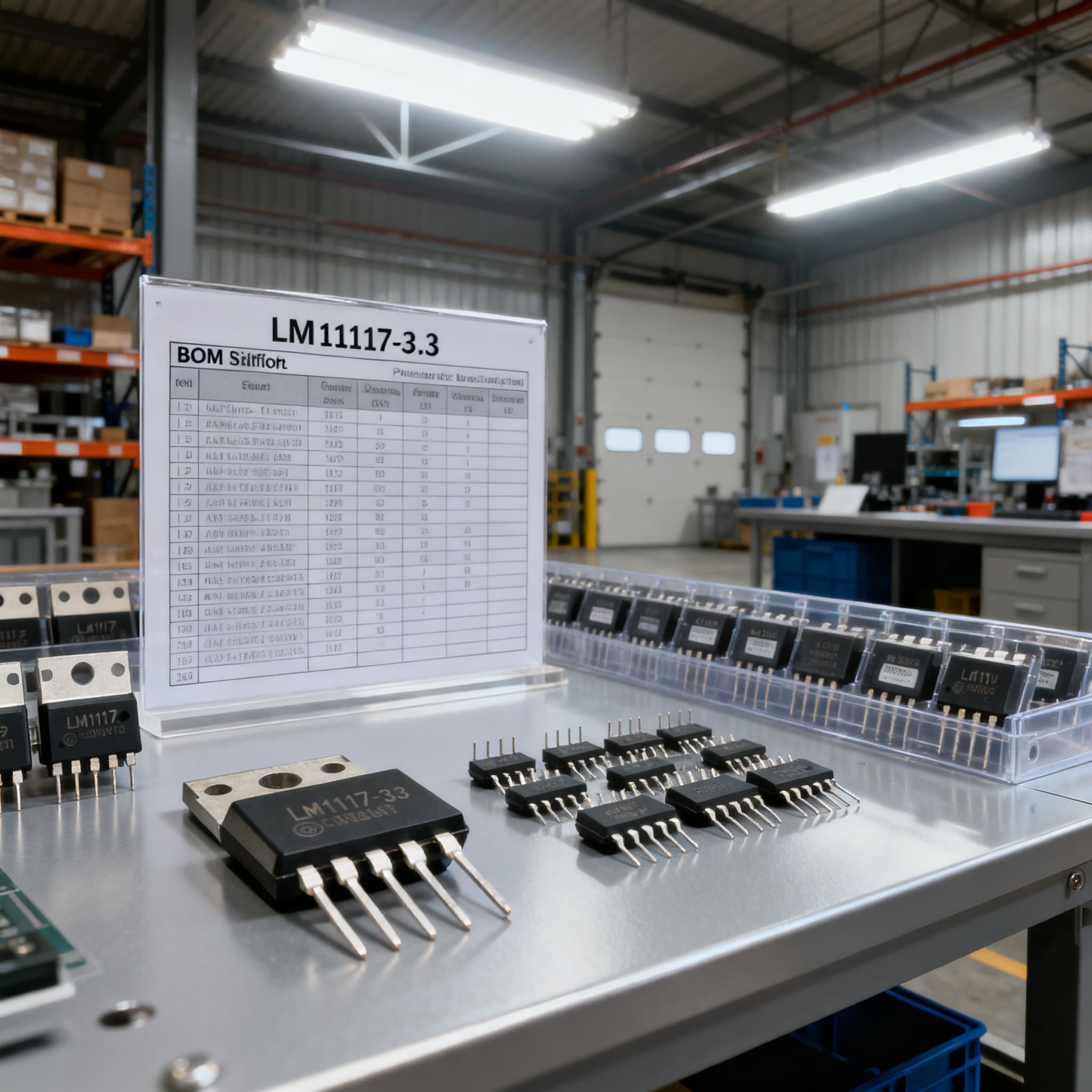
LM1117-3.3 Procurement Guide: Pinout and Spec Checks for RFQ
LM1117-3.3 procurement checklist: datasheet specs and pinout fields to verify on RFQ, plus BOM upload path on BOMNow.
Why a Pinout Check on the LM1117-3.3 Can Save a Production Run
When a line suddenly needs a higher-current regulator, it’s tempting to scan the shelf for a drop-in replacement. The LM317 equivalent guide highlights a trap that has caught more than one procurement team: the LM317 adjustable regulator uses an ADJ–OUT–IN pinout in the popular TO‑220, while the LM1117 family – including the LM1117-3.3 – orders its pins GND–OUT–IN in SOT‑223. Swap them blindly and you’ll route the input voltage straight to the output pin, damaging downstream 3.3 V logic before the production line ever reaches full speed. An RFQ that opens with “LM1117‑3.3 or equivalent” without pinout verification can ship a board‑level short straight into your assembly flow.
Even within the 1117 universe, second‑source data sheets from Cystech and CYStek list the same GND‑OUT‑IN order, but clones occasionally tweak the thermal pad connection or omit the tab entirely in alternate packages. A buyer who doesn’t lock the pinout in the RFQ may receive parts that fit the footprint but connect the heatsink tab to a different net, creating a latent thermal failure. Starting every RFQ for the LM1117-3.3 with a pinout confirmation isn’t just a datasheet formality – it’s the cheapest insurance against a line‑down situation.
LM1117-3.3 Datasheet Decoded: Pinout, Dropout, and What 800 mA Really Means
The LM1117-3.3 is a fixed 3.3 V low‑dropout regulator designed to deliver up to 800 mA of continuous output current. TI’s product page anchors the base specification, while second‑source suppliers like Cystech and CYStek provide compatible parts that often carry a 1 A headline figure. The table below consolidates the critical parameters a buyer must verify before quoting, alongside the fine print that can make or break a design.
| Parameter | TI LM1117-3.3 | Cystech / CYStek LM1117-3.3 | Procurement Notes |
|---|---|---|---|
| Fixed Output Voltage | 3.3 V ±1% (max) | 3.3 V ±1% (max) | Verify accuracy grade; some suffix codes denote tighter tolerance. |
| Guaranteed Output Current | 800 mA | 800 mA (guaranteed); 1 A typical | 1 A operation requires adequate copper area – see thermal derating curves. |
| Dropout Voltage (max) | 1.2 V at 800 mA | 1.3 V at 1 A (CYStek) | 5 V input is safe; 4.5 V input is the absolute floor. |
| Line Regulation | 0.2% max | 0.2% max | Measured over full input voltage range; confirms output stability. |
| Load Regulation | 0.4% max | 0.4% max | From 10 mA to 800 mA; critical for noise-sensitive loads. |
| Quiescent Current | 5 mA typical | 5 mA typical | Increases slightly at full load; budget for battery applications. |
| Thermal Shutdown | 165 °C typical | 150 °C typical | Protection threshold; good faith test for counterfeit detection. |
| Output Capacitor ESR | 0.3 Ω to 22 Ω (tantalum/electrolytic) | 0.3 Ω to 22 Ω (CYStek) | Pure ceramic MLCCs can oscillate; confirm with manufacturer’s datasheet. |
| Package (SOT‑223) | GND–VOUT–VIN (pins 1‑2‑3) | Identical pinout | Heatsink tab is typically VOUT – lock in RFQ. |
Tip: The 800 mA guarantee from TI is conservative. Cystech and CYStek data sheets rate the part at 1 A, but that figure assumes a junction temperature of 25 °C and a generous copper pour. For a real PCB inside a closed enclosure, procurement should treat the 800 mA limit as the safe continuous rating. Always request the thermal derating graph from the specific manufacturer when the BOM calls for currents above 600 mA – a LM1117-3.3 running at 1 A without adequate heatsinking will thermal-cycle itself into early failure.
The pinout is deceptively simple: GND on pin 1, VOUT on pin 2, and VIN on pin 3. But the tab connection varies. In the standard SOT‑223, the tab is internally connected to VOUT, so the copper plane on the PCB acts as a heatsink. The CYStek specification explicitly marks the tab as “VOUT,” while other second sources may leave it ambiguous. Before you send an RFQ, confirm that the quoted part matches this pinout exactly – and that the assembly house knows where to connect the thermal pad.
AMS1117, LD1117, or LT1117: Choosing the Right 3.3V LDO Without a PCB Spin
When the LM1117-3.3 isn’t available in the volumes you need, the SOT‑223 footprint opens the door to several pin‑compatible alternatives. The AMS1117, LD1117, AP1117, and the LT1117 from Analog Devices all share the same GND‑VOUT‑VIN orientation, but they differ in dropout voltage, temperature range, and stability requirements. The table below maps the key trade‑offs so you can decide whether a second source can be approved without a board revision.
| Metric | LM1117-3.3 (TI) | AMS1117-3.3 (AMS) | LD1117-3.3 (ST) | LT1117-3.3 (Analog) | Selection Note |
|---|---|---|---|---|---|
| Pinout (SOT‑223) | GND‑VOUT‑VIN | GND‑VOUT‑VIN | GND‑VOUT‑VIN | GND‑VOUT‑VIN | Identical across all four; a genuine drop‑in footprint. |
| Max Dropout (at rated IOUT) | 1.2 V at 800 mA | 1.3 V at 1 A | 1.2 V at 800 mA | 1.1 V at 800 mA | LT1117 offers the lowest dropout, buy‑ers can use 4.5 V input with confidence. |
| Guaranteed Output Current | 800 mA | 1 A (typical) | 800 mA | 800 mA | AMS1117 often advertised as 1 A; verify thermal conditions. |
| Operating Temperature Range | 0 °C to 125 °C | ‑40 °C to 125 °C | 0 °C to 125 °C | ‑40 °C to 125 °C | AMS1117 and LT1117 suit industrial; TI part needs extended temp suffix. |
| Output Capacitor ESR | 0.3 Ω to 22 Ω (tantalum/electrolytic) | 0.3 Ω to 22 Ω (tantalum/electrolytic) | 0.3 Ω to 22 Ω | 0.3 Ω to 10 Ω (tantalum) | LT1117 tightens ESR range; ceramic possibility depends on exact revision. |
| Adjustable Version Available | Yes (LM1117‑ADJ) | Yes (AMS1117‑ADJ) | Yes (LD1117‑ADJ) | Yes (LT1117‑ADJ) | Adjustable pinout differs from fixed; never assume drop‑in for ADJ variants. |
The AMS1117’s typical application circuit shows a 10 µF tantalum output capacitor, identical to the LM1117, but older AMS1117 data sheets sometimes recommend a 22 µF capacitor for stability. The LT1117, with its reduced dropout, may also accept a ceramic MLCC if the ESR is within the required window – a detail that the LT1117 datasheet clarifies. Procurement teams should not assume that “pin‑compatible” means “capacitor‑compatible.” Include the exact capacitor dielectric and ESR range in the RFQ, and if you plan to qualify a second source, re‑test the stability margin with your actual load.
RFQ-Ready: How to Specify LM1117-3.3 to Avoid Counterfeit and Capacitor Surprises
An RFQ that lists only “LM1117‑3.3” leaves too much room for interpretation. The TI ordering table shows suffixes like M3, MP, and MDT that define the package and temperature grade, while the CYStek spec sheet uses a different coding system. Combine that variability with the capacitor ESR requirement, and you have a recipe for a batch of parts that oscillate or overheat. Use the checklist below to build an RFQ that procurement can execute without back‑and‑forth questions.
| RFQ Field | What to Verify | Why It Matters |
|---|---|---|
| Full MPN | Include suffix: e.g., LM1117MP‑3.3, LM1117MPX‑3.3, LM1117‑3.3M3 | Suffix dictates package, lead finish, and tape‑and‑reel orientation; mismatched suffix can halt placement. |
| Manufacturer & Lifecycle | Confirm “Active” status on TI’s product page; for Cystech/CYStek, request latest PCN. | NRND or EOL parts force last‑time buys; proactive lifecycle check avoids shortages. |
| Package Type | SOT‑223, TO‑252, SOT‑89, or WSON – confirm pin 1 orientation and tab connection. | TO‑252 (DPAK) has different thermal characteristics; SOT‑89 may lack tab altogether. |
| Thermal Pad Connection | Specify “Tab = VOUT” in the line note; request a mechanical drawing. | Prevents assembly house from floating the pad or connecting it to GND, causing thermal run‑away. |
| Output Capacitor ESR | State the required ESR range: 0.3 Ω to 22 Ω (tantalum) or equivalent. | Ceramic capacitors with <0.1 Ω ESR can cause oscillation; the RFQ should align with the design’s capacitor selection. |
| Country of Origin & Lot Code | Request country of origin and batch lot code traceability. | Non‑franchised sources may ship mixed lots; consistent lot codes help isolate field failures. |
| Markings | Cross‑reference the top‑side marking with the manufacturer’s datasheet. | Counterfeit parts often use generic “1117‑33” marking without the manufacturer logo; a quick visual check catches most fakes. |
Once the RFQ is built, procurement can add a few low‑effort verification steps that pay off in assembly reliability:
- Request a sample of 5–10 units from the quoted lot and measure the dropout voltage at the design’s maximum load current. A dropout significantly higher than 1.3 V may indicate a re‑marked lower‑grade regulator.
- Test the thermal shutdown by shorting the output and monitoring the junction temperature; a genuine LM1117-3.3 should shut down before reaching 170 °C.
- Verify the quiescent current at no load; a reading above 10 mA at room temperature warrants a closer look.
- If the RFQ accepts a second‑source alternative, lock the capacitor type and ESR requirement in the line item so the design team can evaluate stability before volume production.
Note: The Cystech datasheet and the CYStek spec show identical electrical characteristics, but the recommended PCB layout can differ slightly. When dual‑sourcing, ask both suppliers for their recommended land pattern and verify that the stencil opening is consistent – a small change in paste volume can tip the thermal balance at 1 A.
LM1117-3.3 Procurement: Pinout, Capacitor, and Sourcing Questions Answered
Q: Is the LM1117-3.3 pinout identical to the AMS1117-3.3 in SOT‑223?
Yes, both use GND–VOUT–VIN (pin 1‑2‑3) in the popular SOT‑223 package. The AMS1117 guide confirms this orientation. However, always verify the datasheet of the specific manufacturer, as some clones may have subtle differences in the thermal pad connection. The tab is typically VOUT on both, but a few second‑source parts tie the tab to GND – a detail that must be confirmed before approving the substitute.
Q: What is the minimum dropout voltage for the LM1117-3.3, and how does it affect my input voltage choice?
The LM1117 guarantees a dropout of 1.2 V max at 800 mA, so a 5 V input is sufficient. The CYStek datasheet confirms a 1.3 V max dropout at 1 A. Using a 3.3 V input is impossible; you need at least 4.5 V. If the design uses a Li‑ion battery that dips to 3.6 V, the regulator will drop out of regulation, and the output will fall below 3.3 V. Procurement should flag this during the RFQ when the input voltage is near the dropout limit.
Q: What output capacitor is required for stability, and can I use a ceramic MLCC?
The LM1117 requires a minimum 10 µF tantalum or electrolytic capacitor on the output with ESR between 0.3 Ω and 22 Ω. A pure ceramic capacitor with low ESR can cause oscillation. The CYStek spec sheet details this requirement; always check the exact manufacturer’s datasheet, as some newer versions may tolerate ceramics. If the design must use MLCCs, add a series resistor to raise the ESR, or consider a modern LDO that is stable with ceramic output capacitors.
Q: How can I verify the authenticity of LM1117-3.3 parts when sourcing from non‑franchised distributors?
Check for consistent laser markings, the manufacturer’s country of origin, and request the lot code. Cross‑reference the part marking with the TI product page or the Cystech datasheet. Test dropout voltage and quiescent current; a counterfeit may exhibit higher dropout or no thermal shutdown. Use the TI OPN (Orderable Part Number) to confirm the exact ordering code. If the lot code dates back more than three years, investigate the supply chain history.
Q: The LM1117-3.3 is listed as ‘active’ by TI, but I see ‘Cystech’ and ‘CYStek’ versions. Should I standardize on one manufacturer?
TI’s LM1117 is the original, but Cystech and CYStek offer compatible second‑source parts. The key is to lock the MPN in your AVL (Approved Vendor List) and include the manufacturer’s full name in the RFQ. The CYStek spec shows identical electrical characteristics, but procurement should still verify the datasheet revision date and PCN status. Standardizing on one manufacturer simplifies incoming inspection, but maintaining a qualified second source reduces supply risk – especially for a high‑volume part like the LM1117-3.3.
References & Further Reading
- TI LM1117 Product Page – official specifications, ordering table, and lifecycle status.
- LM317 Equivalent Guide – explains pinout differences between LM317 and LM1117.
- AMS1117 3.3V Voltage Regulator Guide – pinout, application circuit, and replacement options.
- AMS1117-3.3 Ultimate Guide – detailed pinout, capacitor requirements, and 5V to 3.3V circuit.
- Cystech LM1117-3.3 Datasheet – second‑source electrical characteristics.
- CYStek LM1117-3.3M3 Specification – updated datasheet with thermal pad and capacitor ESR details.
- LT1117/LT1117-3.3 Datasheet – Analog Devices low‑dropout regulator with extended temperature range.
A well‑written RFQ for the LM1117-3.3 eliminates surprises before they reach the pick‑and‑place machine. When you’re ready to consolidate your BOM, Upload Your BOM at BOMNow for a single, consolidated quote. Or request a quote for the LM1117‑3.3 line item alone – our team will confirm pinout, package, and capacitor specs with the supplier so you don’t have to.