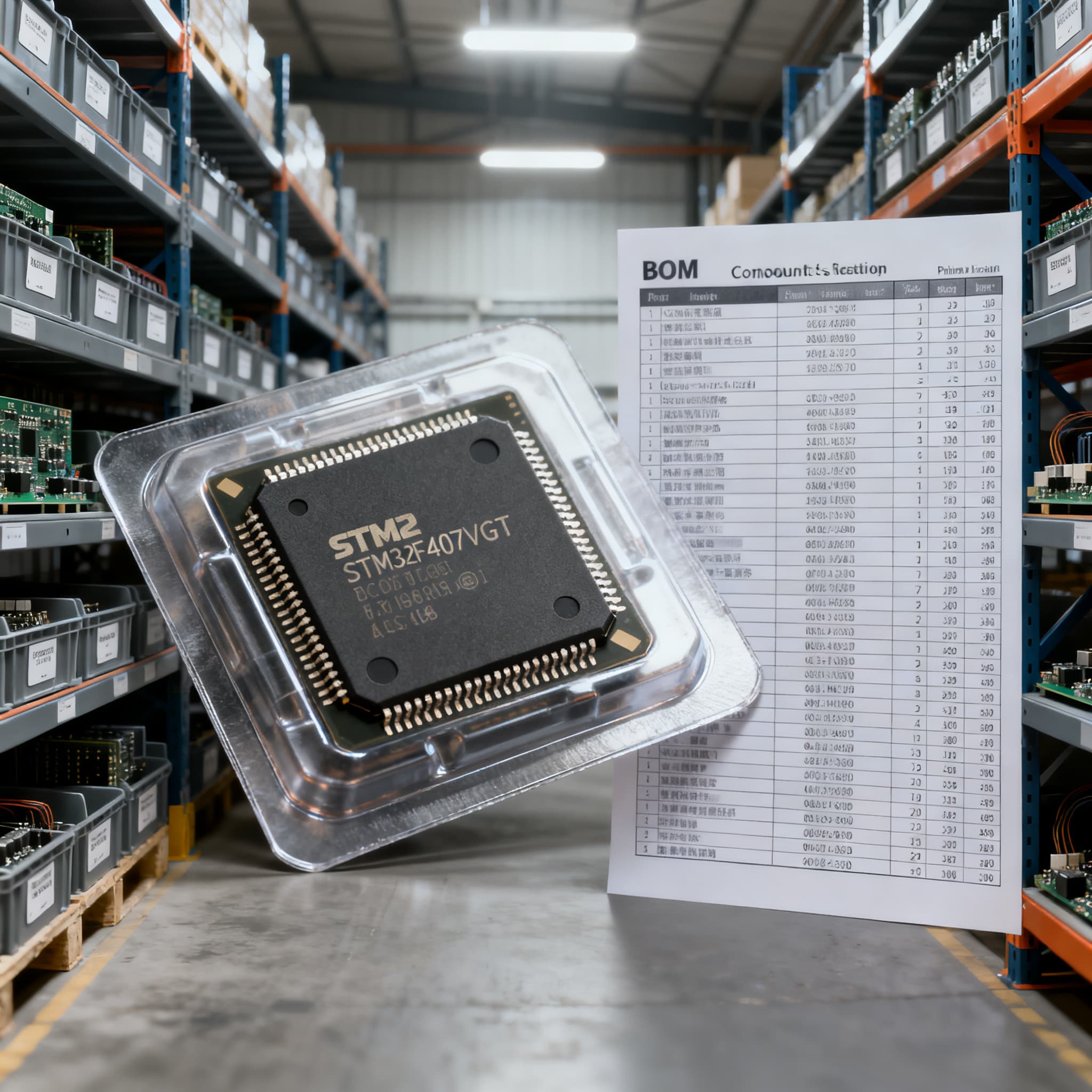
STM32F407VGT6 Procurement Guide: Pinout and Spec Checks for RFQ
STM32F407VGT6 procurement checklist: datasheet specs and pinout fields to verify on RFQ, plus BOM upload path on BOMNow.
STM32F407VGT6 Procurement: Pinout and Spec Checks to Build a Stronger RFQ
Why the STM32F407VGT6 Demands a Pinout‑First RFQ Approach
When a design runs on the STM32F407VGT6, the procurement process is rarely as simple as re‑ordering a commodity op‑amp. This Cortex‑M4 microcontroller sits at the heart of countless industrial IoT gateways, motor drives, and real‑time control systems. Its 1 MB Flash, 192 KB SRAM, and rich peripheral set make it indispensable—and that same indispensability means long allocation cycles, a steady stream of gray‑market substitutes, and a market where a single overlooked pin can derail an entire production batch.
A loose BOM line that reads “STM32F407VGT6” without pin‑level verification acts like an open door for well‑meaning but incompatible substitutions. A supplier might offer a pin‑compatible device with half the Flash, or a third‑party clone whose RMII timing drifts just enough to break Ethernet PHY communication. The result is a field failure that costs far more than the few cents saved on the quote.
Tip: Uploading a multi‑line BOM to BOMNow for consolidated quotes is a strong first step—it puts multiple authorized and vetted sources into one view. But the real guardrail is building the RFQ around the exact pinout, peripheral mix, and marking details your design requires. This article walks through the spec‑checks that turn a generic purchase request into a procurement‑grade specification, helping you reject the wrong parts before they ever reach your reflow oven.
The following sections ground the conversation in the pages of the STM32F407 datasheet and reference manual, map the alternative landscape (including the GD32 clones that frequently appear on spot markets), and provide a practical RFQ template that flags deviations before they become product recalls. Wherever counterfeit risk is a concern, we cross‑reference ERAI’s database, because a lot‑traceable, authorized supply chain is the only safe foundation for a high‑runner like the STM32F407VGT6.
Reading the STM32F407VGT6 Pinout and Datasheet Like a Sourcing Engineer
The STM32F407VGT6 comes in an LQFP‑100 package with 82 user‑configurable I/O pins. Those pins are multiplexed across up to 15 alternate functions, so the same physical pad can carry an FSMC data line, a CAN2 TX signal, or a UART4 RTS flow‑control line depending on the firmware configuration. For a sourcing engineer, the question is not “does the pin count match?” but “which specific peripheral functions are bonded to my design, and will any alternative part remove or re‑time them?”
Start with the critical interfaces. If your board uses the Ethernet MAC in RMII mode, the REF_CLK, TXD[0:1], RXD[0:1], and MDIO pins must map exactly to the RMII‑dedicated pins (typically PA1, PA2, PA7, PC1, PC4, etc.). The STM32F407VGT6 integrates a full‑speed USB OTG PHY, so the DP and DM pins (PA12, PA11) are fixed; a substitute that lacks an internal PHY would require a costly board re‑spin. The FSMC peripheral, often used for external SRAM or LCD controllers, consumes 24–32 data/address lines that overlap with GPIOs on PD, PE, and PF ports—replacing the part with a pin‑compatible but functionally different MCU can silently break the memory map.
Before drafting an RFQ, compile a checklist of must‑have parameters from the latest ST datasheet. The table below captures the core electrical and resource profile that separates the STM32F407VGT6 from lower‑memory variants or clones.
| Parameter | STM32F407VGT6 Value | Notes / RFQ Relevance |
|---|---|---|
| Package | LQFP‑100 (14 × 14 mm) | Pin‑1 orientation, pad footprint. Verify with supplier’s photo. |
| Core / Max Frequency | ARM Cortex‑M4F @ 168 MHz | FPU and DSP instructions; clock tree must match reference. |
| Flash Memory | 1 MB | Firmware size check; any lower‑density substitute will brick the application. |
| SRAM | 192 KB (128 + 64 KB CCM) | Stack/heap allocation; 64 KB core‑coupled memory for time‑critical routines. |
| Operating Voltage (VDD) | 1.8 V to 3.6 V | Internal regulator; VCAP pins require 2.2 µF ceramic capacitors. |
| Temperature Range | –40 °C to +85 °C | Industrial grade; confirm marking suffix “VGT6” (not VGT6TR or VGT6H). |
| Ethernet MAC | 10/100 Mbit/s with RMII/MII | No integrated PHY; verify RMII reference clock pin assignment. |
| USB OTG | Full‑speed (12 Mbit/s) with integrated PHY | High‑speed mode requires external ULPI PHY. |
| CAN / SPI / I2C | 2× CAN, 3× SPI, 3× I2C | Multiplexed with GPIO; confirm which instance your design uses. |
| BOOT Configuration | BOOT0 pin (with optional BOOT1 via PB2) | Must be strapped per reference manual; wrong pull‑up/down prevents boot. |
Beyond the electrical specs, the oscillator pins (PH0‑OSC_IN, PH1‑OSC_OUT) and NRST pin have strict layout requirements. The NRST pin expects a 100 nF capacitor to ground, and the BOOT0 pin must be pulled low through a 10 kΩ resistor for normal flash boot. If you receive a batch of microcontrollers whose reset behavior deviates from the ST datasheet, the firmware may not start, and the fault can be maddeningly intermittent. Including these details in the RFQ—not just the MPN—makes it clear that the supplier is expected to deliver a part that matches the reference specification, not just a footprint‑compatible object.
STM32F407VGT6 Alternatives: When to Evaluate Pin‑Compatible and Cross‑Family Options
When the STM32F407VGT6 sits on allocation, procurement teams often look to the broader STM32F407 family or third‑party clones. The most common “pin‑compatible” alternative is the STM32F407VET6, housed in the same LQFP‑100 package but with 512 KB Flash and 128 KB SRAM—half the resources of the VGT6. The pinout is identical, so a contract manufacturer may not flag the swap, but the firmware will immediately fault if the binary size exceeds the smaller memory map. The STM32F407ZGT6 steps up to a 144‑pin package; it adds more I/O but is not drop‑in compatible without a board change.
Outside the ST ecosystem, the GD32F407VGT6 from GigaDevice is a frequent sight on the open market. While it mimics the Cortex‑M4 core and many peripherals, its flash controller timing, PLL lock characteristics, and DMA behavior can differ in ways that are invisible during a pin‑continuity test but catastrophic in a real‑time control loop. Several manufacturing support forums have documented Ethernet PHY link‑drop issues when GD32 clones are substituted without thorough firmware re‑validation.
The table below compares the contenders. Use it to guide your engineering team’s validation plan before accepting any alternative.
| Comparison Metric | STM32F407VGT6 (Reference) | STM32F407VET6 (Lower‑Density) | GD32F407VGT6 (Clone) | Selection Note & Failure Boundary |
|---|---|---|---|---|
| Package | LQFP‑100 | LQFP‑100 | LQFP‑100 | Footprint matches; functional compatibility is not guaranteed. |
| Flash / SRAM | 1 MB / 192 KB | 512 KB / 128 KB | 1 MB / 192 KB (nominal) | VET6 fails if firmware > 512 KB; GD32 may have different wait‑state timings. |
| Max Core Frequency | 168 MHz | 168 MHz | 168 MHz (advertised) | Verify PLL lock time and jitter margin; GD32 may require clock tree retune. |
| Ethernet MAC | Yes, RMII/MII | Yes, RMII/MII | Yes, RMII/MII | GD32: watch for REF_CLK timing drift; ST parts are golden reference. |
| USB OTG PHY | Integrated FS PHY | Integrated FS PHY | Integrated FS PHY (claimed) | Test VBUS detection and DP/DM crossover thresholds; clone may miss edge cases. |
| Counterfeit Risk | Low when sourced from authorized distributors | Low (authorized) | High on open market; re‑marking common | Always check ERAI and request lot traceability. |
If a substitute is unavoidable, the engineering team must re‑run the full peripheral test suite—especially for timing‑critical interfaces like RMII, CAN, and FSMC. A simple board‑bring‑up test is insufficient. Download the latest STM32F407 reference manual and compare the alternate‑function table against the GD32F407 equivalent. The pin‑mux differences may be subtle, but they can break a design if a critical UART or timer channel moves to a different pad.
Writing an RFQ That Catches Deviations: Pinout, Marking, and Lifecycle Checks
A well‑constructed RFQ does more than request a price; it makes the supplier’s obligations explicit. For the STM32F407VGT6, the RFQ should attach a one‑page specification sheet that captures the exact MPN, the pin‑level critical function list, and the marking requirements. This sheet becomes the yardstick against which any substitution is judged.
Below is a practical RFQ‑addendum table that you can tailor to your design. It converts the pin‑out and spec checks into clear, supplier‑actionable fields.
| RFQ Element | Specification Guidance | Why It Matters |
|---|---|---|
| Exact MPN | STM32F407VGT6 (no generic “STM32F407” or family suffix substitution) | Prevents memory‑size or peripheral downgrades. |
| JTAG/SWD Pinout | PA13 (SWDIO), PA14 (SWCLK), plus optional NRST and SWO; must be available after reset | Debugger connection essential for firmware validation; some clones remap SWD pins. |
| BOOT0 Strap | BOOT0 pulled low through 10 kΩ for flash boot; BOOT1 (PB2) as per design | Incorrect strap leads to boot‑to‑ROM or startup failure. |
| NRST Circuit | 100 nF capacitor to GND; no external pull‑up required (internal pull‑up) | Noise or wrong cap value causes spurious resets. |
| Marking Format | ST logo, “STM32F407VGT6”, date code (YYWW), trace code, pin‑1 dimple | Non‑standard font or missing pin‑1 indent is a red flag for re‑marking. |
| Lot Traceability | Full lot number and date code; request photograph of top‑side marking | Enables verification against ERAI and ST’s authorized distribution records. |
| Lifecycle Status | Currently Active (verify with ST product page at time of order) | NRND or EOL parts should be flagged; do not accept unconfirmed stock. |
| Deviation Notice | Supplier must flag any deviation from the above in writing before shipment | Prevents silent substitution; documented acceptance protects your production. |
Pair this RFQ addendum with a BOM upload on BOMNow. The platform consolidates quotes from multiple sources, and when you attach the specification sheet, you ensure that every quoting supplier responds to the same clear requirements. For any batch sourced outside the authorized channel, make it a policy to cross‑reference the lot codes against ERAI’s counterfeit database before payment. A photo of the top‑side marking, examined under magnification for font consistency and the correct pin‑1 dimple, is a quick but powerful filter.
STM32F407VGT6 Procurement FAQ: What Engineers and Buyers Need to Know
The following questions reflect the day‑to‑day challenges that arise when sourcing the STM32F407VGT6 for high‑mix, low‑volume production or volume builds.
Q: What’s the actual difference between STM32F407VGT6 and STM32F407VET6, and can I substitute one for the other?
A: The VGT6 has 1 MB Flash and 192 KB SRAM, while the VET6 delivers 512 KB Flash and 128 KB SRAM. Both use the identical LQFP‑100 package and pinout, so a substitution is electrically invisible until the firmware tries to access memory beyond the VET6’s limit. If your binary exceeds 512 KB or the stack/heap allocation requires the full SRAM, the VET6 will fail. Always verify the firmware’s memory footprint and stack usage before accepting the smaller part, and never assume a pin‑compatible upgrade is a drop‑in.
Q: Does the STM32F407VGT6 include a built‑in Ethernet MAC and USB OTG PHY?
A: Yes, the chip integrates a 10/100 Mbit/s Ethernet MAC with RMII/MII interface and a full‑speed USB OTG peripheral with an integrated full‑speed PHY. For USB high‑speed operation, you still need an external ULPI PHY. Confirm that the RMII_REF_CLK pin (usually PA1) and the USB_DP/DM pins (PA12, PA11) match your board’s routing; a substitute that moves these functions to different pads will break both interfaces even if the part is otherwise pin‑compatible.
Q: How can I verify that a batch of STM32F407VGT6 is genuine and not a relabeled part?
A: Start with a visual inspection under a microscope: the ST logo should be crisp, the date code font consistent with known genuine parts, and the pin‑1 orientation dimple well‑defined. Next, read the electronic signature via the debug port—the Cortex‑M4 DBGMCU and unique device ID (UID) registers should match the expected device ID for the STM32F407 family. Finally, cross‑reference the lot code with ERAI’s database. Authorized distributors can also provide certificates of conformance; if you are buying from the open market, make ERAI verification a non‑negotiable step before release.
Q: What’s the safest way to specify the NRST and BOOT0 pins in the RFQ to avoid boot failures?
A: Explicitly require that BOOT0 be pulled low through a 10 kΩ resistor and that NRST have a 100 nF capacitor to ground, exactly as the reference manual specifies. This is a design‑side requirement, but including it in the RFQ communicates that the supplied part must behave within the accepted reset timing and boot‑level thresholds. If a substitute part has a different internal pull‑up or reset threshold, the firmware may not start. Request a schematic snippet in the quote to confirm the supplier understands the constraint.
Q: Why does the STM32F407VGT6 often appear with long lead times, and what should I do?
A: The STM32F407VGT6 is a workhorse in industrial automation, motor control, and IoT gateways—markets that consume vast quantities and compete for the same fab allocation. It is not unusual for lead times to stretch beyond 20 weeks during allocation cycles. Rather than react to one shortage, upload your entire BOM to BOMNow to receive multi‑source quotes that include authorized distributors. Avoid spot‑market purchases without ERAI verification, and wherever possible, maintain a safety stock of pre‑verified parts to buffer against allocation swings.
Q: Are there any pin conflicts between the FSMC and GPIO when using the STM32F407VGT6?
A: Yes, many FSMC address/data lines share pins with GPIO and other peripherals. For instance, FSMC data lines (D0–D15) occupy many pins including PD0, PD1, PD14, PD15, and PE7–PE15, which can conflict with CAN2 and UART4 if those peripherals are needed that would otherwise be available on those pins. If your design relies on CAN2 or UART4 alongside the FSMC, you must map them to alternate pins, if available, or accept the conflict. In your RFQ, highlight which peripheral sets are critical so that the sourcing team can reject any pin‑compatible but functionally incompatible alternative. Substituting a part that rearranges the FSMC pin‑mux will break the memory interface immediately.
References & Further Reading
- BOMNow — BOM Sourcing — Upload a BOM for consolidated electronic component quotation.
- STM32F407VGT6 on BOMNow — Product landing page for the exact MPN.
- STM32F407VGT6 Datasheet (STMicroelectronics) — Electrical characteristics, pinouts, and package information.
- STM32F407 Reference Manual (RM0090) — Alternate function mapping, reset, and clock tree.
- STM32F407VG Product Page (ST) — Lifecycle status, ordering codes, and tools.
- ERAI — Counterfeit and high‑risk electronics reporting database.
- STM32F407VGT6 on Digi‑Key — Authorized distributor listing with parametric data.
- STM32F407VGT6 on Mouser — Another authorized source for reference.
Ready to build a stronger RFQ? Upload your multi‑line BOM to BOMNow and receive consolidated quotes from multiple sources, or request a single‑MPN quote for the STM32F407VGT6 with the pin‑level specification sheet attached. That way, every supplier understands exactly what you need—before a single part is shipped.